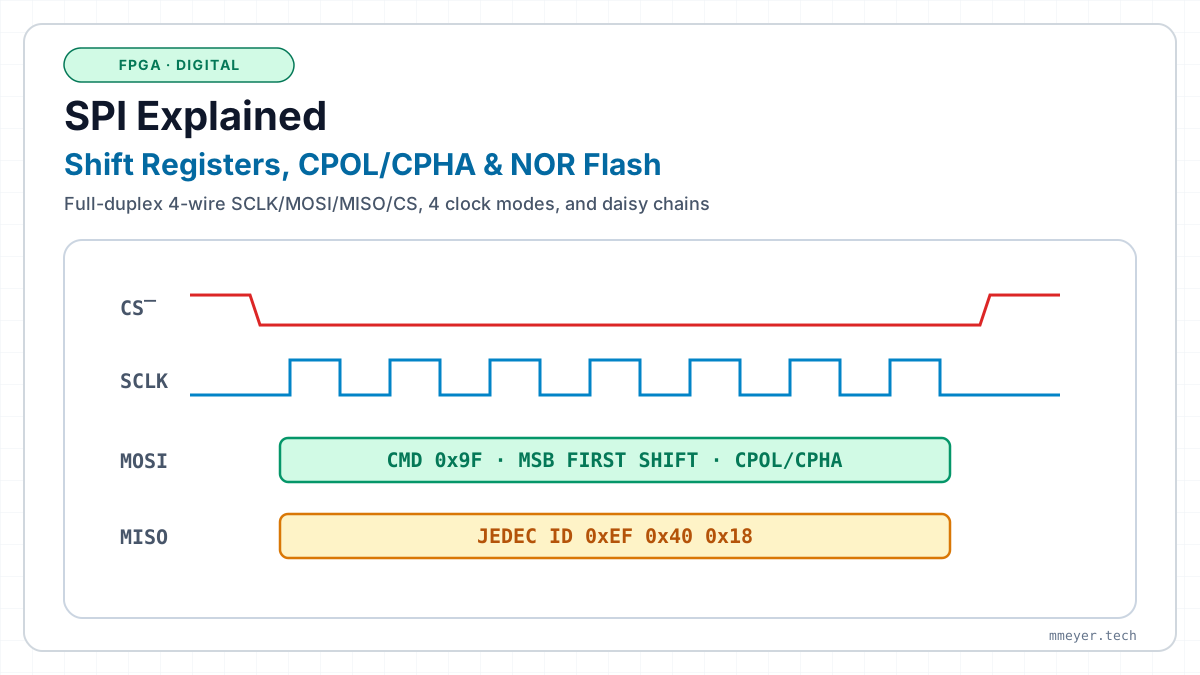
SPI explained: shift registers, chip select, CPOL/CPHA, commands, flash, daisy chains and timing
An interactive guide for people who have never looked at an SPI bus. Every step loads a scenario into a small simulator of a real 4-wire bus: one controller, an accelerometer, a serial NOR flash and a chain of two 74HC595-style shift registers, each with its own chip select. Move through time tick by tick and watch the wires, the waveform, the decoded bytes and the state inside every chip. The playground lets you build your own transfers, including broken ones: wrong modes, missing chip selects, glitches, MISO that arrives too late, two chips talking at once.
SPI Explained Edge by Edge: Shift Registers, Chip Select, CPOL/CPHA Modes, NOR Flash and Timing
Step through every SCLK edge of the Serial Peripheral Interface: circular MOSI/MISO shift registers, active-low CS framing, SPI Modes 0 through 3, multi-byte W25Q128 Flash commands, daisy chained peripherals, Dual/Quad SPI, and setup/hold timing analysis.