The diode: a one-way valve made from two kinds of silicon
A diode lets current through in one direction and blocks it in the other. This chapter shows why, starting from the doped silicon of chapter 5: how a junction forms all by itself, what its band diagram looks like, where the exponential current–voltage curve comes from, and what happens at breakdown, during switching, and when light is involved (LEDs, photodiodes, solar cells). It ends with the circuit inside every power supply: the rectifier.
You need: doping and the Fermi level (chapter 5, section 7), band diagrams across a device (chapter 5, section 8), voltage and current (chapter 1). Next: chapter 7 uses the same junctions as source and drain of a transistor.
Current one way, almost nothing the other way
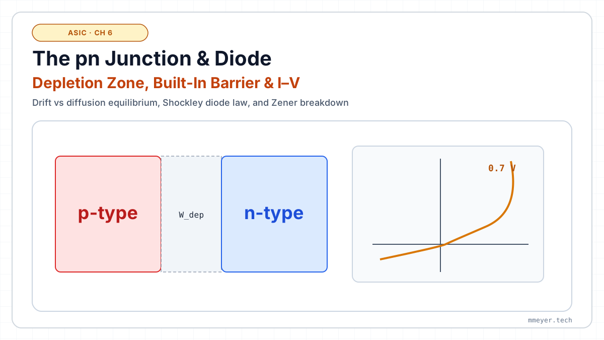
The circuit symbol is a triangle pointing in the direction in which (conventional) current may flow, ending in a bar. The triangle side is the anode (the p side), the bar is the cathode (the n side). In the forward direction a silicon diode starts to conduct at about 0.6–0.7 V. In the reverse direction it blocks, up to its breakdown voltage (section 5).
A good picture is a check valve in a water pipe: a flap that opens when the water pushes from one side and closes when it pushes from the other. A weak spring holds the flap shut until the pressure exceeds a small threshold, the diode's ~0.6 V. Below, a sine voltage drives current through a diode and a 1 kΩ resistor. Only the positive half-waves get through.
A diode is not a resistor. There is no fixed R = U/I: the current grows exponentially with the voltage (section 4). That is why the output follows the input minus an almost constant ~0.6 V once the diode conducts, and why small diodes are used as nearly ideal switches.
Diffusion, recombination, and a field that stops them
Start with two separate pieces (chapter 5, section 7). Both are electrically neutral: in the p piece each mobile hole is balanced by a fixed negative acceptor ion; in the n piece each mobile electron by a fixed positive donor ion. Now press them together:
- Diffusion. Electrons wander from the crowded n side into the p side, holes the other way, just as ink spreads in water. Nobody pushes them; it is pure random motion from where there are many to where there are few.
- Recombination. An electron that meets a hole falls into it. Both disappear.
- Uncovered ions. Near the junction the fixed ions lose their partners: a layer of negative acceptors on the p side and positive donors on the n side. This is the depletion region, also called the space-charge region.
- The field. The ion layers create an electric field pointing from n to p. It pushes electrons back towards n and holes back towards p: a drift current against the diffusion.
- Equilibrium. Within picoseconds, drift and diffusion cancel exactly. What remains is a built-in voltage of about 0.7 V across the junction, with no current.
A cartoon with a few hundred particles: random walk plus drift in the field of all charges, recombination when an electron meets a hole. A real junction holds about 10¹⁶ ions per cm³ and reaches equilibrium in picoseconds.
Why does the field not keep growing? Each carrier that crosses uncovers more ions and makes the field stronger, which makes the next crossing harder. The process stops when the hill in the band diagram is just high enough that the few carriers still climbing it are balanced by the few minority carriers rolling down. That is exactly the statement "EF is flat in equilibrium" from chapter 5.
Band diagram, charge, field and potential, computed live
Bring p-type and n-type silicon into contact. Electrons diffuse from the n side, where there are many, into the p side; holes go the other way; they meet and recombine. What stays behind near the junction are the dopant ions, which cannot move: positive donors on the n side, negative acceptors on the p side. This depletion region (almost no free carriers, but full of fixed charge) carries an electric field that pushes back against further diffusion. Equilibrium is reached when EF is flat. The bands then bend by the built-in voltage:
The shape of the bend follows from Poisson's equation: charge → field → potential → bands, one integration at a time. In the depletion approximation the charge is a block of −qNA and a block of +qND, the field is a triangle, the potential two parabolas, and the total width is
An applied voltage V separates the two quasi-Fermi levels by qV. Forward bias (p side positive) lowers the hill by qV, and the number of electrons with enough energy to climb it grows like eqV/kT: ten times more per 60 mV. Reverse bias raises the hill. Then only the few minority carriers that happen to reach the junction roll down it: a tiny, constant saturation current I0.
Electrons on the n side sit at Ec with a thermal spread of a few kT. Only those in the exponential tail above the barrier cross: that is the diode's exponential. On the reverse side, an occasional electron is thermally generated in the p region and rolls down the hill: the saturation current, independent of the bias. The quasi-Fermi levels are drawn schematically; they merge again within a diffusion length.
The diode equation, and what real diodes add to it
Section 3 explained the ideal diode: the current is set by how many carriers get over the hill, and that number grows with eqV/kT. With the thermal voltage VT = kT/q = 25.9 mV at 300 K:
- I0, the saturation current, is tiny (here 10⁻¹⁴ A). It contains ni², so it rises steeply with temperature: about a factor of two every 5 K. At constant current the forward voltage therefore drops by about 2 mV per kelvin; this is how many chips measure their own temperature.
- n, the ideality factor, is 1 for the ideal diffusion current. At small currents, recombination inside the depletion region adds a second current with n ≈ 2. On a log scale the curve then bends from 120 mV per decade to 60 mV per decade.
- Series resistance Rs (contacts, neutral regions) takes over at large currents: the curve bends away from the straight line because part of the voltage drops across Rs.
On the log scale an exponential becomes a straight line: the slope tells the ideality factor directly (60 mV per decade means n = 1). Engineers read diode data sheets exactly like this.
When the blocking direction gives up: avalanche and Zener
In reverse bias the hill gets higher and the depletion region wider. Only the tiny saturation current flows, until the field in the junction becomes so strong that one of two mechanisms sets in:
Breakdown is not destructive by itself: a Zener diode (the name is used for both mechanisms) is operated in breakdown on purpose, as a voltage reference. Diodes rated around 5–6 V mix both mechanisms, and their opposite temperature drifts nearly cancel. Damage only happens when the current is not limited and the junction overheats.
A diode stores charge, and needs time to get rid of it
Two kinds of charge make a diode behave like a capacitor:
- Junction capacitance. The depletion region is an insulator between two conducting sides: a capacitor whose plate distance W changes with the voltage. For an abrupt junction . Reverse-biased diodes used as voltage-tuned capacitors are called varactors.
- Stored (diffusion) charge. In forward bias, injected minority carriers fill the neutral regions before they recombine after the lifetime τ. The stored charge is Q = τ·I, giving a diffusion capacitance Cd = τI/(nVT).
When a conducting diode is suddenly reverse-biased, the stored charge must first be pulled out. Until it is gone, the junction stays forward-biased and a large reverse current flows. Only then does the diode block. This storage time follows from the charge-control model:
Fast-recovery and Schottky diodes exist for exactly this reason. A Schottky diode is a metal–semiconductor contact: the current is carried by majority carriers flowing over a barrier, so no minority charge is stored. It also has a lower forward voltage (~0.3 V), which makes it the diode of choice in switching power supplies.
LEDs turn current into light, photodiodes and solar cells do the reverse
In a forward-biased diode, injected electrons recombine with holes. The energy released is about the band gap Eg. In a direct-gap material (GaAs, InGaN) it leaves as a photon of wavelength
That is a light-emitting diode. In silicon, with its indirect gap (chapter 9, section 13), an electron at the bottom of the conduction band and a hole at the top of the valence band have different crystal momenta. A photon carries almost no momentum, so light emission needs help from a lattice vibration and is very rare; the energy becomes heat instead. The reverse process works in any semiconductor: a photon with energy above Eg creates an electron–hole pair, the junction field separates them, and a photocurrent IL flows. Run without external supply, the illuminated diode is a solar cell:
White LEDs are blue InGaN LEDs coated with a yellow phosphor. The 2014 Nobel Prize in Physics went to the inventors of the efficient blue LED. A crystalline silicon solar cell of 10 cm × 10 cm delivers about 0.6 V and 4 A in full sun; modules connect dozens of cells in series.
From alternating to direct current
Every mains power supply starts with diodes that turn AC into DC. A half-wave rectifier uses one diode and passes only the positive half-waves. A bridge rectifier uses four diodes so that both half-waves charge the output, always through two diodes in series. A smoothing capacitor fills the gaps: it is charged in short, strong current pulses at the peaks and discharges into the load in between. The remaining wobble is the ripple:
Look at the diode current: the capacitor recharges only during a short window near each peak, so the diodes carry pulses several times larger than the average load current. That is why rectifier diodes and transformers must be rated for much more than the DC current suggests.
The diode in one table
| Idea | Formula | Typical silicon numbers |
|---|---|---|
| built-in voltage | 0.6–0.9 V | |
| depletion width | 0.05–5 µm | |
| diode equation | ×10 per 60 mV (n = 1) | |
| temperature | VF drops ≈ 2 mV/K | |
| avalanche breakdown | 6 V … kV | |
| junction capacitance | pF range | |
| storage time | ns to µs | |
| LED wavelength | GaAs 870 nm, InGaN 450 nm | |
| solar cell | ≈ 0.6–0.7 V per cell | |
| rectifier ripple | halve it with a bridge |
Next: chapter 7. A MOSFET contains two of these junctions, source and drain, with a gate in between that decides whether current may pass.
Every term on this page
| anode, cathode | p side and n side of a diode; forward current flows from anode to cathode |
| forward / reverse bias | p side positive / negative with respect to the n side |
| diffusion, drift | motion from high to low concentration; motion pushed by an electric field |
| recombination | an electron falls into a hole; both disappear |
| depletion (space-charge) region | zone without mobile carriers, filled with fixed ionized dopants |
| built-in voltage Vbi | the potential step across the junction in equilibrium |
| quasi-Fermi levels | separate Fermi levels for electrons and holes when a voltage is applied |
| saturation current I0 | the tiny reverse current; scale factor of the diode equation |
| thermal voltage VT | kT/q = 25.9 mV at 300 K |
| ideality factor n | 1 for diffusion current, about 2 for recombination in the depletion region |
| series resistance | resistance of contacts and neutral regions, important at high current |
| avalanche / Zener breakdown | carrier multiplication by impact ionization / band-to-band tunneling |
| junction capacitance, varactor | capacitance of the depletion region; a diode used as a voltage-tuned capacitor |
| minority-carrier lifetime τ | average time before an injected minority carrier recombines |
| storage time, reverse recovery | time a switched-off diode keeps conducting backwards while its stored charge leaves |
| Schottky diode | metal–semiconductor diode: majority carriers only, fast, ~0.3 V forward |
| direct / indirect gap | band edges at the same / different crystal momentum; only direct-gap materials make efficient LEDs |
| LED, photodiode, solar cell | current → light; light → current (reverse bias); light → power (no bias) |
| Voc, Isc, fill factor | open-circuit voltage, short-circuit current, Pmax/(VocIsc) of a solar cell |
| rectifier, ripple | circuit turning AC into DC; the remaining periodic variation of the output |