nMOS and pMOS: how a MOSFET works, its curves and its formulas
The MOSFET (metal–oxide–semiconductor field-effect transistor) is the switch and the amplifier inside every chip; a processor contains billions. This chapter builds it in three steps: the structure and the sign conventions, the MOS capacitor that controls the silicon surface, and the complete transistor with its band diagram. Then it collects the formulas engineers use every day: regions of operation, threshold voltage and body effect, channel-length modulation, subthreshold slope, the small-signal model, the capacitances, and what changes in short-channel transistors. nMOS and pMOS side by side.
You need: the pn junction (chapter 6), band bending (chapter 5, section 8), capacitors and Ohm's law (chapter 1). Next: chapter 8 wires nMOS and pMOS together into CMOS logic.
Four terminals, two flavours
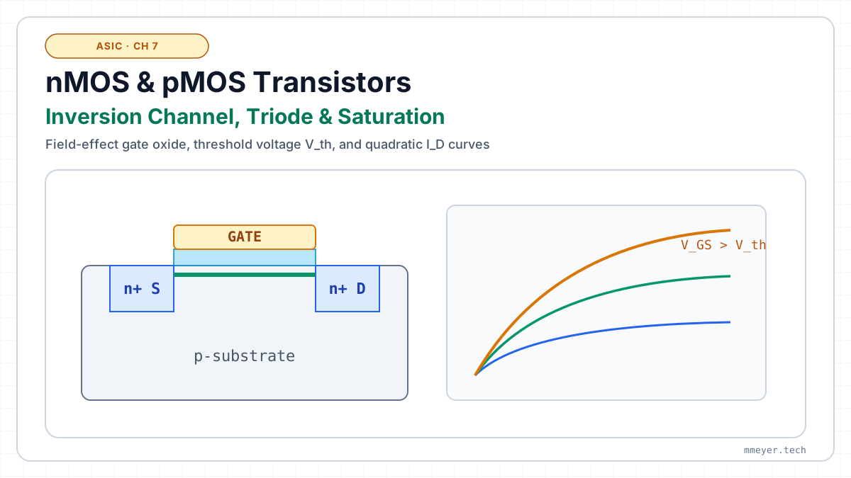
A MOSFET has four terminals. The gate (G) sits on a thin insulating oxide and never conducts DC current. The source (S) is where the carriers come from, the drain (D) where they leave. The body or bulk (B) is the silicon underneath, usually tied to the source or to the supply. All voltages are measured from the source: VGS, VDS, VBS. The drain current ID is counted positive when it flows into the drain.
| nMOS | pMOS | |
|---|---|---|
| body | p-type (the substrate) | n-type (an n-well) |
| source and drain | n⁺ | p⁺ |
| carriers in the channel | electrons, μn ≈ 250–500 cm²/Vs in the channel | holes, μp about 2–3 times lower |
| threshold voltage | VTn > 0 (typically 0.2–0.7 V) | VTp < 0 (typically −0.2 to −0.7 V) |
| turns on when | VGS > VTn: gate above the source | VGS < VTp: gate below the source |
| source is the terminal at | the lower potential | the higher potential |
| drain current ID | positive | negative |
The pMOS is the mirror image of the nMOS: every doping type, voltage and current changes sign. Electrons in an nMOS roll down the band edge; holes in a pMOS float up. All formulas below therefore come in pairs, and you can always write the pMOS version with magnitudes: VSG, VSD, |VTp| and |ID|.
Gate, oxide, silicon: accumulation, depletion, inversion
Now the heart of every transistor: a gate electrode (metal or heavily doped poly-silicon), a thin oxide (SiO₂: band gap ≈ 9 eV, a barrier of 3.1 eV for electrons and ≈ 4.7 eV for holes) and the p-type silicon body. No current flows through the oxide. The gate acts on the silicon only through the electric field, like one plate of a capacitor.
| Term | Meaning |
|---|---|
| vacuum level | energy of an electron at rest just outside the material |
| work function Φ | energy to lift an electron from EF to the vacuum level (gate: Φm, silicon: Φs) |
| electron affinity χ | energy from Ec to the vacuum level (Si 4.05 eV, SiO₂ ≈ 0.95 eV, so the oxide barrier is 3.1 eV) |
| flat-band voltage VFB | (Φm − Φs)/q: the gate voltage that makes the silicon bands flat (no oxide charge assumed) |
| Fermi potential φF | (kT/q)·ln(NA/ni): how far EF lies below Ei in the bulk |
| surface potential ψs | how far the bands bend down at the surface, in volts |
Raise the gate voltage VG on p-type silicon:
- Accumulation (VG < VFB): the negative gate attracts holes, which pile up at the surface. Bands bend up.
- Flat band (VG = VFB): no charge anywhere, bands flat.
- Depletion (VFB < VG < VT): holes are pushed away and leave the negative acceptor ions behind. Bands bend down. At ψs = φF, Ei crosses EF at the surface: "mid-gap".
- Inversion (VG > VT): the bands bend so far that at the surface EF is closer to Ec than to Ev. Electrons, the minority carriers, gather in a sheet a few nm thick: the surface has turned n-type. Strong inversion starts at ψs = 2φF, where the surface is as n-type as the bulk is p-type. The gate voltage there is the threshold voltage:
The silicon side is computed exactly (Poisson–Boltzmann, no depletion approximation). The field at depth where the bands are bent by ψ is
The first bracket belongs to the holes and acceptors, the second to the electrons. The surface charge is Qs = −εsℰ(ψs), and the gate voltage splits into the work-function difference, the band bending in the silicon and the drop across the oxide: . The oxide is drawn much wider than it really is.
Interface traps
The Si/SiO₂ interface is not perfect. Broken (dangling) bonds create states inside the gap, the interface traps, with a density Dit per cm² and per eV. Like all states they are filled up to EF. The standard picture: traps in the upper half of the gap are acceptor-like (neutral when empty, negative when filled), traps in the lower half donor-like (positive when empty, neutral when filled). In accumulation EF sits low at the surface, so the donors between EF and Ei are empty and positive. At mid-gap all traps are neutral. In inversion the acceptors between Ei and EF are filled and negative. The gate must supply this trapped charge as well, so the C–V curve stretches out along the voltage axis.
Reading the C–V curve. The measured capacitance is Cox in series with the silicon's own capacitance Cs = −dQs/dψs. In accumulation the holes respond right at the surface: C ≈ Cox. In depletion the charge changes at the edge of a growing depletion layer: C drops. In inversion it depends on the frequency. At low frequency (quasi-static) the inversion electrons follow the signal and C climbs back to Cox. At high frequency (~1 MHz) minority carriers cannot be generated fast enough, only the depletion edge moves, and C stays at its minimum. In the usual high-frequency picture the traps do not follow the AC signal either, but they still stretch the curve, because they take up charge whenever the DC bias changes.
A transistor is a gate-controlled barrier
Add two heavily doped n⁺ regions, source and drain, on either side of the MOS capacitor. For an electron leaving the source, the path to the drain is n⁺–p–n⁺: the p region under the gate, with its high Ec, is a barrier, like a dam. The gate controls the height of that dam.
- Off (VGS well below VT): the barrier is high. Only the far Boltzmann tail of the source electrons gets over. Current ≈ 0.
- Subthreshold (VGS < VT): the gate lowers the barrier by qΔVGS/n (n ≈ 1.2–1.5, because part of the gate voltage drops across the oxide). The current grows exponentially, ten times for every . Because of this Boltzmann tail, no conventional transistor at room temperature can switch more steeply than 60 mV per decade.
- On (VGS > VT): the barrier is gone and an inversion layer, the channel, connects source and drain. For small VDS it is a gate-controlled resistor (linear region). Once VDS exceeds about (VGS − VT)/n, the channel is pinched off at the drain end and the current saturates: electrons reaching the pinch-off point roll down the steep drop into the drain like water over a weir.
Model: charge-sheet model (Brews), one formula for subthreshold, linear and saturation: ID = μn(W/L)∫(−Qi)dV along the channel, with the inversion charge Qi from the surface-potential equation of section 2. Device: n⁺ poly gate, tox = 4 nm, NA = 10¹⁸ cm⁻³, W/L = 10 µm / 1 µm, μn = 300 cm²/Vs, giving VT ≈ 0.57 V. A long-channel device: short-channel effects are ignored. The band diagram follows Ec along the silicon surface; the dashed orange line is the electron quasi-Fermi level, which falls by qVDS from source to drain.
Regions of operation and the formulas for hand calculations
The charge-sheet model of section 3 is accurate but needs a computer. For hand calculations engineers use the square-law model, with three regions. Its parameters: the process transconductance k' = μCox (set by the factory), the aspect ratio W/L (chosen by the designer), the threshold VT, and the overdrive Vov = VGS − VT.
- Triode (linear) region: the channel reaches from source to drain. For small VDS it is a resistor R = 1/(k'(W/L)Vov) whose value the gate sets.
- Saturation: the channel is pinched off at the drain end; the current depends on VGS but hardly on VDS. Pinch-off point moving towards the source shortens the channel a little, so the current still creeps up: channel-length modulation, λ ≈ 0.02–0.2 V⁻¹ (larger for short transistors).
- Body effect: a body below the source (VSB > 0) widens the depletion layer, so the gate must hold more charge before inversion: with the body-effect coefficient γ = √(2qεsNA)/Cox.
- Subthreshold: below VT the current is not zero but falls exponentially, 10× per S ≈ 70–100 mV (section 3).
Check yourself: the boundary between triode and saturation is the parabola VDS = VGS − VT. On the right, √ID is a straight line in saturation; where it hits zero is the threshold voltage. That is how VT is measured. Switch to pMOS: the same curves appear in the third quadrant, because VDS, VGS and ID are all negative.
The transistor as an amplifier
For analog circuits the transistor sits at a fixed operating point (Q) and small signals ride on top. Near Q the curves are straight lines, so small changes obey linear equations:
The transconductance gm is the slope of the transfer curve, the output resistance ro the inverse slope of the output curve in saturation, and gmro the intrinsic gain, the largest voltage gain one transistor can give. In a common-source amplifier a resistor RD from the supply to the drain turns the current change into a voltage change: .
Increase the input amplitude: the output gets lopsided. The small-signal model is a tangent; it only holds while the swing stays small compared with the overdrive voltage.
Why switching takes time: the gate is a capacitor
To switch a transistor, its gate charge must change. The total gate capacitance is about CoxWL, but how it is shared between source, drain and body depends on the region (Meyer model):
- Cutoff: no channel. The gate couples to the body: Cgb ≈ CoxWL in accumulation, smaller in depletion.
- Triode: the channel touches both ends: Cgs ≈ Cgd ≈ ½CoxWL.
- Saturation: the channel is pinched off at the drain: Cgs ≈ ⅔CoxWL, Cgd ≈ 0.
- Plus the overlap capacitance CovW where the gate overlaps source and drain, and the junction capacitances of source and drain to the body (chapter 6, section 6).
In an amplifier, Cgd connects input and output. Because the output swings Av times more than the input, Cgd looks (1 + |Av|) times larger from the input: the Miller effect, often the main speed limit of an amplifier.
What changes when the channel is only a few dozen nanometres long
- Velocity saturation. Electron speed stops growing with the field at about vsat ≈ 10⁷ cm/s. The saturation current then rises roughly linearly with Vov instead of quadratically: .
- DIBL (drain-induced barrier lowering). The drain field reaches the source end of the channel and lowers the barrier of section 3: VT drops when VDS rises, and the off-current grows.
- Worse subthreshold swing and more leakage, because the gate loses control over the channel to source and drain.
- The cure is better electrostatics: thinner (high-k) gate dielectrics, then gates wrapped around the channel: FinFETs (gate on three sides, since 2011) and gate-all-around nanosheets (since about 2022).
Illustrative model: currents per µm of width with tox,eq = 1.5 nm, μ = 300 cm²/Vs, vsat = 10⁷ cm/s; DIBL and subthreshold swing grow with an assumed exponential dependence on L. Real values depend strongly on the technology.
nMOS and pMOS formulas side by side
| quantity | nMOS | pMOS |
|---|---|---|
| on condition | VGS > VTn | VSG > |VTp| |
| threshold | ||
| triode | ||
| saturation | ||
| overdrive, saturation condition | Vov = VGS − VTn, VDS ≥ Vov | Vov = VSG − |VTp|, VSD ≥ Vov |
| body effect | same for |VTp| with VBS | |
| subthreshold | ||
| small signal | ||
| capacitances | ||
| mobility | k'n/k'p = μn/μp ≈ 2–3, so a pMOS needs to be 2–3 times wider for the same current | |
Next: chapter 8 puts one nMOS and one pMOS in series and gets a logic gate that uses power only while it switches.
Every term on this page
| MOSFET | metal–oxide–semiconductor field-effect transistor |
| gate, source, drain, body | control electrode on the oxide; where carriers enter; where they leave; the silicon underneath |
| enhancement mode | off at VGS = 0, turned on by the gate (all logic transistors) |
| threshold voltage VT | gate voltage where strong inversion starts and the channel forms |
| overdrive Vov | VGS − VT, how far the gate is above threshold |
| k', W/L, β | μCox; channel width over length; β = k'W/L |
| triode (linear) region | VDS < Vov: channel from source to drain, gate-controlled resistor |
| saturation, pinch-off | VDS ≥ Vov: channel ends before the drain, current nearly independent of VDS |
| channel-length modulation λ | slight rise of the saturation current with VDS |
| body effect γ | threshold rises when the source is above the body |
| subthreshold swing S | gate voltage per decade of current below threshold, ≥ 60 mV at 300 K |
| operating point, small signal | the DC bias; small variations around it |
| transconductance gm | ∂ID/∂VGS, current change per gate-voltage change |
| output resistance ro, intrinsic gain | 1/(λID); gmro, the maximum gain of one transistor |
| common-source amplifier | input at the gate, output at the drain with a load RD; gain −gm(ro ∥ RD) |
| Meyer capacitances, overlap, Miller effect | region-dependent split of the gate charge; gate–source/drain overlap; Cgd amplified by the gain |
| velocity saturation | carrier speed limited to ~10⁷ cm/s at high fields |
| DIBL | drain-induced barrier lowering: VT falls with VDS in short transistors |
| FinFET, gate-all-around | 3D transistors whose gate surrounds the channel on three or four sides |