CMOS logic: two complementary switches that make every digital chip
CMOS (complementary metal–oxide–semiconductor) logic uses nMOS and pMOS transistors in pairs, so that in every steady state one of them is off and no current flows from the supply to ground. This chapter starts with transistors as switches, builds the inverter, measures its noise margins, shows how two inverters store a bit, builds NAND, NOR and complex gates, and ends with delay, power and the reason why supply voltages stopped shrinking.
You need: nMOS and pMOS and their curves (chapter 7). Next: chapter 9 goes one level deeper and derives the band picture from quantum mechanics. Digital systems built from these gates continue in the digital track (buses, clock-domain crossing, verification).
nMOS passes a strong 0, pMOS passes a strong 1
In digital circuits a MOSFET is a voltage-controlled switch. An nMOS closes when its gate is high (logic 1 = VDD), a pMOS closes when its gate is low (logic 0 = 0 V). But they are not equally good at passing every level. An nMOS can pull a node all the way down to 0 V, but when it tries to pass a 1 the output only rises until the transistor's own VGS = VDD − Vout shrinks to about VT: it stops near VDD − VT, a weak 1. The pMOS is the mirror image: a strong 1 and a weak 0 that stops near |VTp|. Hence the CMOS rule: pMOS pull up, nMOS pull down. A transmission gate, an nMOS and a pMOS in parallel, passes both levels well.
The output node is a 10 fF load capacitor that starts at the opposite level. Currents come from the charge-sheet transistor model of chapter 7 (body effect ignored, which would make the weak levels even weaker).
nMOS + pMOS: a switch that only draws power while it switches
The pMOS transistor is the mirror image: an n-type body (an n-well in the p-substrate), p⁺ source and drain, and holes in the channel. It turns on when its gate is low, VGS < −|VT|. In band language: a negative gate bends the bands up at the surface until the holes, floating up like bubbles, form a channel. Holes are about three times less mobile than electrons, so pMOS transistors are usually made wider.
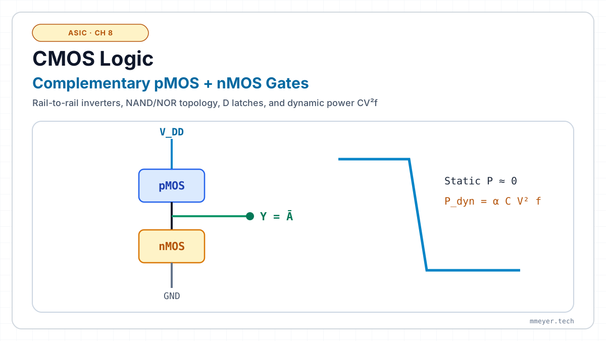
CMOS (complementary MOS) puts one of each in series between the supply VDD and ground. The two gates form the input, the two drains the output:
- Input low: pMOS on, nMOS off → the output is connected to VDD: high.
- Input high: nMOS on, pMOS off → the output is pulled to ground: low.
- In both steady states one transistor is off, so there is no path from VDD to ground. Only the tiny subthreshold leakage flows. Energy is needed when the output switches: one full charge-and-discharge cycle of the load capacitance C draws C·VDD² from the supply. Half of it is lost as heat in the pMOS while charging; the stored half is lost in the nMOS while discharging.
α is the fraction of clock cycles in which the node switches, f the clock frequency. Billions of these inverters, and their cousins NAND and NOR (section 4), make up every processor.
The current spikes only appear on edges: on the rising output edge the pMOS charges the load from VDD; on the falling edge the nMOS dumps it to ground. In between, the supply current is practically zero. With Wp/Wn = 1 the weaker pMOS shifts the switching point below VDD/2 and slows the rising edge; at about 3, matching the mobility ratio, the inverter is symmetric.
How much noise a gate tolerates, and how two inverters store a bit
Real signals pick up noise between gates. The transfer curve defines four voltages: the guaranteed output levels VOH and VOL, and the input levels VIL and VIH where the curve's slope is −1 (beyond them, noise would be amplified). The noise margins say how much noise a 1 or a 0 can carry and still be read correctly by the next gate:
Connect two inverters in a ring and plot both transfer curves in the same graph, one mirrored: the butterfly plot. The curves cross three times. The two outer crossings are stable: the ring holds a 0 or a 1 for as long as the supply is on. This latch is the heart of every SRAM cell, register and flip-flop. The middle crossing is unstable, like a ball on top of a hill: the metastable state. Start the latch there and watch it fall to one side; the closer you start to the middle, the longer the decision takes. That is the reason for synchronizers in clock-domain crossings.
NAND, NOR and any other function from series and parallel switches
A CMOS gate has two networks: a pull-up network of pMOS transistors between VDD and the output, and a pull-down network of nMOS transistors between the output and ground. Switches in series conduct only if all of them are on (AND); switches in parallel conduct if any one is on (OR). The two networks are duals: wherever the nMOS are in series, the pMOS are in parallel, and vice versa. That guarantees that for every input combination exactly one network conducts, so the output is always driven and no current flows straight through.
- NAND2: two nMOS in series (output low only if A and B are both 1), two pMOS in parallel. 4 transistors.
- NOR2: two nMOS in parallel, two pMOS in series. Also 4 transistors, but the series pMOS are slow (low hole mobility), so designers prefer NAND.
- CMOS gates are naturally inverting: AND = NAND + inverter (6 transistors). Complex gates such as AOI21, Y = ¬(A·B + C), implement a whole expression in one stage.
- NAND alone is universal: every Boolean function can be built from NAND gates only (the same holds for NOR).
How fast, how hungry, and why the supply voltage stopped shrinking
A gate's propagation delay tp is the time its transistor needs to move the charge CL·VDD of the next gates' inputs and wires with its on-current Ion. A clock cycle must fit a chain of such delays (here 25 gates). Power has two parts: dynamic power for charging and discharging, and leakage, the subthreshold current Ioff of the transistors that are supposed to be off. Ioff grows ten-fold for every S ≈ 85 mV that VT is lowered (the subthreshold swing of chapter 7).
Lowering VDD saves energy quadratically but makes the gates slower; near VT the delay explodes, the slow cycles let leakage add up, and the energy per cycle has a minimum. Lowering VT instead makes the gates fast again but raises leakage exponentially.
Illustrative chip: 10⁸ gates, CL = 2 fF per gate including wires, Ion = 100 µA at 0.7 V overdrive (alpha-power law with exponent 1.3), subthreshold swing 85 mV/decade.
Dennard scaling (1974) was the recipe of four decades of progress: shrink all dimensions and all voltages by the same factor κ, and every transistor becomes κ times faster and needs κ² less power, while κ² more of them fit on the same area. The power per area stays constant:
| quantity | dimensions, VDD, VT | C, I | delay | power per gate | gates per area | power per area |
|---|---|---|---|---|---|---|
| factor | 1/κ | 1/κ | 1/κ | 1/κ² | κ² | 1 |
Around 2005 this broke down. VT cannot follow, because the subthreshold swing cannot fall below 60 mV per decade at room temperature (chapter 7): every 60 mV less threshold means at least ten times more leakage. So VDD got stuck near 0.7–1 V, power density rose, and clock frequencies plateaued at 3–5 GHz. Since then performance has come from parallelism (many cores), specialised blocks, better transistors (FinFET, gate-all-around) and parts of the chip that are switched off when idle ("dark silicon").
Flip-flops, layout, latch-up, and on to the digital track
Flip-flops. Two latches from section 3, a master and a slave, open in opposite clock phases. Together they capture the input exactly at the clock edge and hold it for a whole cycle: an edge-triggered D flip-flop, the building block of registers, counters and state machines. The input must be stable a short setup time before and a hold time after the edge. If it changes inside that window, the latch starts near its balance point and can stay metastable for a while, exactly the slow decision you saw in section 3.
Layout. Gates are drawn as standard cells of equal height: a VDD rail along the top, a ground rail along the bottom, pMOS in the n-well near VDD, nMOS near ground, and polysilicon or metal gate lines crossing both. Ten or more metal layers above the transistors wire billions of cells together.
Latch-up. Bulk CMOS hides an unwanted four-layer p-n-p-n structure: pMOS source (p⁺), n-well, p-substrate, nMOS source (n⁺). It forms two parasitic bipolar transistors that feed each other, like a thyristor. A current spike can trigger it, and then it shorts VDD to ground until the power is removed. Designers prevent it with well and substrate contacts (taps) close to every transistor, which keep the base resistances Rwell and Rsub small, with guard rings, or with insulating (SOI) substrates.
Latch-up: the collector current of each parasitic transistor is the base current of the other. Short taps (small Rwell, Rsub) keep both bases at their rail and break the loop.
Up the stack. With flip-flops and gates you can build anything digital: processors, memories and the interfaces that connect chips. The digital track continues there: from a plugged-in cable to TCP, the serial buses SPI and I²C, the on-chip bus AXI4-Lite, a host controller bridging SPI to AXI, safe clock-domain crossing (where metastability matters most) and verification with UVM.
CMOS on one page
| idea | key fact | formula or number |
|---|---|---|
| switches | nMOS passes a strong 0, pMOS a strong 1 | weak levels VDD − VT and |VTp| |
| inverter | one transistor always off: no static current | energy per cycle C·VDD² |
| noise margins | slope −1 points of the transfer curve | NMH = VOH − VIH, NML = VIL − VOL |
| latch | two inverters in a ring store one bit | decision time ≈ τ·ln(VDD/ΔV) |
| gates | pull-up and pull-down networks are duals | NAND2, NOR2: 4 transistors each |
| speed | charge CLVDD moved by Ion | tp ≈ 0.69 CLVDD/Ion |
| power | switching plus leakage | P = αNCVDD²f + NVDDIoff |
| scaling | VT cannot drop below ~0.2–0.3 V: Dennard scaling ended | S ≥ 60 mV/decade at 300 K |
Where next? Chapter 9 derives the band diagrams behind all of this from quantum mechanics. Chapter 10 uses quantum tunneling and electron spin to sense magnetic fields, and chapter 11 stores charge on floating gates.
Every term on this page
| CMOS | complementary MOS: logic built from nMOS and pMOS pairs |
| VDD, GND | supply voltage (logic 1) and ground (logic 0) |
| strong / weak level | a level a transistor passes completely / only up to a threshold drop |
| transmission gate | nMOS and pMOS in parallel, passes both levels well |
| transfer curve (VTC), switching threshold VM | Vout as a function of Vin; the input where Vout = Vin |
| VIL, VIH, VOL, VOH | input levels at the slope −1 points; output levels there |
| noise margin | noise a logic level can carry and still be read correctly |
| latch, butterfly plot | two cross-coupled inverters storing a bit; their two transfer curves in one graph |
| metastability, regeneration time constant τ | the latch balancing between 0 and 1; the time scale on which it escapes |
| SRAM cell | a latch plus two access transistors: one bit of fast memory |
| flip-flop, setup and hold time | edge-triggered storage from two latches; the window around the edge where the input must be stable |
| pull-up / pull-down network | pMOS network to VDD / nMOS network to ground |
| dual network | series and parallel swapped; guarantees exactly one network conducts |
| NAND, NOR, AOI | NOT-AND, NOT-OR, AND-OR-INVERT gates |
| propagation delay tp | time from an input edge to the 50 % point of the output edge |
| activity factor α | fraction of clock cycles in which a node switches |
| dynamic power, leakage power | for charging capacitances; from currents of off transistors |
| Dennard scaling | shrinking dimensions and voltages together at constant power density |
| dark silicon | chip area that must stay switched off to respect the power budget |
| standard cell | a pre-drawn gate layout of fixed height |
| latch-up, tap, guard ring | parasitic thyristor short between VDD and ground; contacts and rings that prevent it |